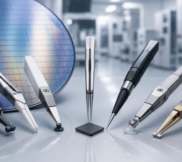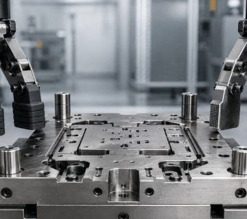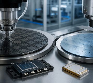
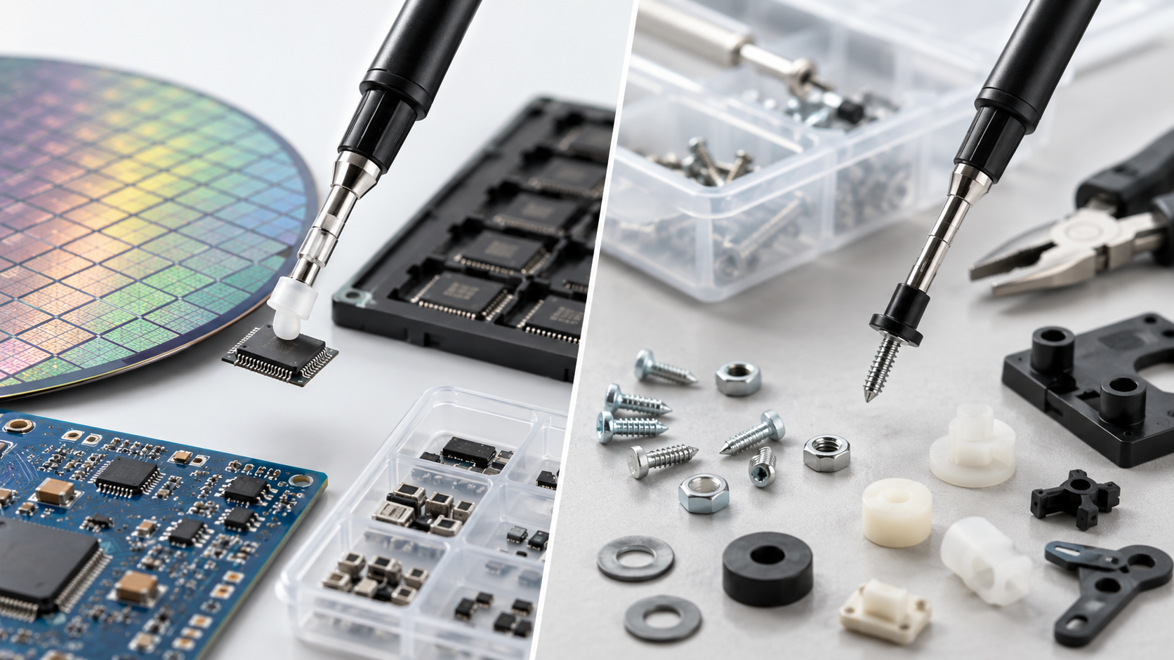
A pick up tool may sound like a simple device for lifting and moving small objects, but the requirements can vary considerably depending on the application.
A general-purpose vacuum pick up tool may be used manually to handle electronic components, jewellery, optical parts or other small objects. In semiconductor manufacturing, however, a pick up tool is a precision production component used to lift, transfer and accurately place fragile semiconductor dies during automated assembly.
Both may rely on vacuum suction, but they differ significantly in precision, materials, dimensions, surface contact, machine compatibility and manufacturing tolerances.
This guide explains the differences between semiconductor pick up tools and normal pick up tools, and why selecting the correct tool matters in precision die-bonding processes.
What Is a Pick Up Tool?
A pick up tool is a device designed to lift, hold, move and release an object without requiring conventional mechanical gripping.
Vacuum-based pick up tools create negative pressure between the tool tip and the object surface. This allows the component to remain attached while it is moved to another position.
The basic principle is used in many industries, including:
- Semiconductor manufacturing
- Electronics assembly
- Laboratories
- Optical component handling
- Jewellery
- Watchmaking
- Precision assembly
- Hobby and repair work
General-purpose products are often supplied as handheld vacuum pens with interchangeable suction cups. Semiconductor versions are usually integrated into die-bonding or pick-and-place equipment and manufactured according to highly specific die dimensions and process requirements.
What Is a Semiconductor Pick Up Tool?
A semiconductor pick up tool is a precision die-bonding tool designed to pick up a semiconductor die, hold it securely during transfer and place it onto a substrate, leadframe or package.
It may also be referred to as a:
- Die pick up tool
- Die collet
- Pick up collet
- Vacuum pick up tool
- Die bonding tool
- Pick up tip
Vacuum is commonly used to hold the die against the tool during transfer. The geometry of the tip is designed to match the die dimensions, surface characteristics and bonding process.
Unlike a handheld vacuum pen, the semiconductor tool forms part of a controlled manufacturing process where placement accuracy, die protection and repeatability are critical.
What Is a General-Purpose Pick Up Tool?
A general-purpose pick up tool is typically designed for manual handling of small components.
Common examples include vacuum pens used for:
- SMD components
- IC packages
- Small electronic parts
- Optical components
- Jewellery
- Watch parts
- Laboratory samples
- Small flat objects
These tools are usually operated by hand and may use an integrated pump, external vacuum supply or manually activated suction mechanism.
For example, commercially available vacuum pens are designed to lift components such as SMDs without requiring tweezers, while other general vacuum tools are used across electronics, optics and precision manual assembly.
Their objective is usually convenient and damage-free manual handling, rather than micron-level automated placement.
Semiconductor Pick Up Tool vs Normal Pick Up Tool
The biggest differences come from the level of precision required.
| Factor | Semiconductor Pick Up Tool | General Pick Up Tool |
|---|---|---|
| Main purpose | Automated die pick-up and placement | Manual handling of small objects |
| Typical application | Semiconductor assembly | Electronics, laboratory, jewellery and repair |
| Precision | Very high | General handling precision |
| Tool dimensions | Application-specific | Standard interchangeable tips |
| Component size | Semiconductor dies and micro-components | Wider range of small objects |
| Materials | Carbide, rubber, plastic, ceramic, high-temperature polymers | Plastic, rubber or silicone tips |
| Vacuum control | Integrated with production equipment | Manual or portable vacuum source |
| Placement repeatability | Critical | Usually operator-dependent |
| Surface protection | Engineered for die condition | General anti-scratch handling |
| Customisation | Frequently customised | Usually standard sizes |
| Machine compatibility | Essential | Usually standalone |
| Production environment | Automated semiconductor line | Manual bench or workshop use |
Although both tools may use suction, semiconductor manufacturing places much stricter demands on the contact surface, material and dimensional accuracy.
1. Precision Requirements Are Much Higher in Semiconductor Manufacturing
The most important difference is precision.
A general vacuum pen only needs to securely lift an object and allow an operator to place it in approximately the correct location.
A semiconductor pick up tool must repeatedly pick and position dies during high-speed production while maintaining controlled alignment.
Semiconductor dies may be extremely small, thin or fragile. A poorly matched tool can contribute to:
- Die cracking
- Chipping
- Scratching
- Placement errors
- Unstable vacuum
- Die rotation
- Surface damage
For this reason, pick up tool geometry is often designed specifically around the die dimensions and bonding process.
2. Semiconductor Pick Up Tools Use Specialised Materials
General vacuum tools commonly use soft suction cups made from rubber or silicone because they need to handle a variety of everyday components.
Semiconductor tools use a much wider range of engineered materials.
Common options include:
- Tungsten carbide
- Rubber
- High-temperature rubber
- Engineering plastics
- Ultem
- Vespel
- Ceramic
- Metallic materials
Small Precision Tools, for example, specifies semiconductor vacuum pick-up tools in rubber, plastic, metallic, tungsten carbide and ceramic materials. Leader HiTech also supplies carbide, rubber and high-temperature pick-up solutions for die-bonding applications.
The correct material depends on factors such as:
- Die surface
- Operating temperature
- Required durability
- Contact pressure
- Die thickness
- Production speed
A hard carbide tool may provide excellent wear resistance, while a softer rubber collet may be preferable where minimising contact damage is the priority.
3. Surface Contact Must Be Carefully Controlled
In general handling, a suction cup only needs enough contact area to lift the object securely.
In semiconductor manufacturing, contact geometry can influence die quality.
The pick up tool must provide sufficient vacuum sealing while avoiding sensitive areas such as:
- Active die surfaces
- Bond pads
- Bumps
- Fine structures
- Coated surfaces
Some tools use flat faces, while others use cavities, grooves or specially shaped contact areas.
A correctly designed semiconductor pick up tool distributes contact and vacuum force appropriately for the die being handled.
This is one reason why a standard vacuum tip cannot simply replace a semiconductor die collet.
4. Semiconductor Tools Must Match the Die Size
General-purpose vacuum pens usually provide several interchangeable suction cups.
An operator selects a cup that appears suitable for the part.
Semiconductor production requires much tighter matching.
Important dimensions may include:
- Die length
- Die width
- Die thickness
- Pick-up surface area
- Vacuum-hole dimensions
- Tool outer diameter
- Shank dimensions
A die pick up tool may therefore be designed specifically for a particular semiconductor package or die.
Leader HiTech’s die-bond tooling includes rubber, carbide and other pick-up tool options designed for different chip and process requirements.
5. Vacuum Performance Is More Critical
Both semiconductor and general-purpose tools use vacuum, but the process requirements differ.
A handheld vacuum pen may simply need enough suction force to prevent a component from falling.
During semiconductor production, vacuum performance must remain consistent across repeated high-speed cycles.
Too little vacuum may cause:
- Dropped dies
- Die movement
- Placement instability
Excessive or poorly distributed force may increase the risk of damaging fragile components.
The vacuum hole, tool face and internal geometry therefore need to work together with the die-bond machine’s vacuum system.
Semiconductor die-attach references describe vacuum as the mechanism used to hold the die inside the collet or pick-up tool while it is transferred to the substrate or die pad.
6. Semiconductor Pick Up Tools Are Designed for Automation
Most general pick up tools are controlled directly by an operator.
The person:
- positions the vacuum pen,
- picks up the component,
- moves it,
- places it,
- releases the vacuum.
Semiconductor tools operate differently.
The pick up tool is installed on automated equipment such as:
- Die bonders
- Die sorters
- Flip-chip machines
- Pick-and-place systems
- Semiconductor packaging equipment
The machine controls movement, vacuum, position and placement timing.
The tool must therefore meet the mounting and dimensional requirements of the equipment being used.
7. Production Temperature Can Affect Tool Selection
A standard handheld vacuum pen usually operates near room temperature.
Semiconductor die-bonding processes may involve elevated temperatures.
This creates additional requirements for:
- Material stability
- Heat resistance
- Dimensional stability
- Vacuum performance
High-temperature pick up tools and specialised polymer collets are available for these applications. Leader HiTech, for example, identifies Vespel collets as suitable for high-temperature use.
This is another reason why general-purpose suction tips may not be suitable for semiconductor production.
8. Semiconductor Tools Often Require Customisation
General vacuum tools are typically purchased in standard configurations.
Semiconductor tooling is frequently customised.
A custom pick up tool may be required when the die has:
- Unusual dimensions
- Sensitive surface structures
- Limited contact areas
- Bumps
- Special coatings
- Non-standard geometry
- Specific temperature requirements
Customisation may involve:
- Tip dimensions
- Vacuum-hole configuration
- Contact profile
- Tool material
- Shank dimensions
- Surface finish
The design should be based on the actual die and equipment requirements rather than simply selecting the closest standard size.
Pick Up Tool Materials in Semiconductor Applications
Different materials serve different manufacturing requirements.
Rubber Pick Up Tools
Rubber collets are widely used because their softer contact surface can reduce the risk of mechanical damage to delicate dies.
They are suitable for many semiconductor die pick-and-place applications. Rubber collets are commonly described by precision-tool manufacturers as one of the most widely used semiconductor pick-up solutions.
Tungsten Carbide Pick Up Tools
Carbide provides:
- High hardness
- Wear resistance
- Dimensional stability
- Long tool life
It can be suitable for die sorting and other applications where durability is important.
However, because carbide is much harder than rubber, contact geometry and process conditions must be carefully controlled to avoid damaging sensitive die surfaces.
Engineering Plastic Pick Up Tools
Materials such as Ultem and Vespel provide an intermediate option between soft rubber and hard metallic or carbide tools.
They may be selected for applications requiring:
- Reduced surface contact risk
- Higher temperature performance
- Good dimensional stability
- Specialised semiconductor handling
Ceramic Pick Up Tools
Ceramic materials may also be used where specialised wear, thermal or electrical characteristics are required. Semiconductor tool manufacturers offer ceramic alongside metallic, plastic, rubber and carbide options.
When Is a Normal Vacuum Pick Up Tool Sufficient?
A general vacuum tool can be suitable when:
- Components are being manually inspected
- Placement accuracy is operator-controlled
- Production speed is not critical
- Parts have relatively robust surfaces
- Tool dimensions do not need to match a specific die
- The task involves prototype, repair or laboratory work
Examples include manually handling:
- SMD components
- IC packages
- small lenses
- watch parts
- laboratory samples
Portable vacuum pens are specifically marketed for this type of work.
When Is a Semiconductor Pick Up Tool Required?
A precision semiconductor pick up tool becomes important when:
- Dies are being handled automatically
- High placement accuracy is required
- The component is fragile
- Die dimensions are very small
- High production repeatability is required
- Process temperatures are elevated
- Surface contact must be carefully controlled
- The tool must interface with a die bonder or sorting machine
In these environments, the tool should be selected as part of the die-bond process rather than treated as a generic vacuum accessory.
How to Choose a Semiconductor Pick Up Tool
Before selecting a tool, semiconductor manufacturers should consider several process parameters.
Die Dimensions
Provide the exact:
- length
- width
- thickness
These determine the appropriate tool face and vacuum configuration.
Die Surface
Identify whether the surface contains:
- bond pads
- bumps
- coatings
- sensitive structures
The contact area should avoid damaging critical features.
Operating Temperature
High-temperature bonding processes may require specialised rubber or engineering polymer materials.
Required Tool Material
Material selection should balance:
- durability
- temperature resistance
- surface protection
- process life
Machine Model
The pick up tool must match the holder and mechanical interface of the die-bond equipment.
Application
Specify whether the tool will be used for:
- Die bonding
- Die sorting
- Flip-chip
- LED assembly
- Tape-and-reel
- Inspection
- Other semiconductor processes
Providing this information helps a tooling supplier determine whether a standard or custom pick up tool is more appropriate.
Frequently Asked Questions
What is a semiconductor pick up tool?
A semiconductor pick up tool is a precision tool used to lift, hold, transfer and place semiconductor dies during die bonding, sorting or packaging processes. Vacuum is commonly used to hold the die during transfer.
Is a die collet the same as a pick up tool?
The terms are often used interchangeably in semiconductor manufacturing. A die collet is a type of pick up tool designed specifically for handling semiconductor dies.
What is the difference between a semiconductor pick up tool and a vacuum pen?
A vacuum pen is typically a handheld general-purpose device used to manually move small components. A semiconductor pick up tool is a precision machine-mounted component designed for automated die handling and highly repeatable placement.
What materials are semiconductor pick up tools made from?
Common materials include rubber, tungsten carbide, engineering plastics, metallic materials and ceramic. The correct choice depends on die sensitivity, temperature, durability and process requirements.
Why are rubber pick up tools commonly used?
Rubber provides a softer contact surface that can help protect fragile semiconductor dies while maintaining sufficient vacuum grip.
When should a carbide pick up tool be used?
Carbide may be suitable where wear resistance, dimensional stability and long service life are priorities, such as certain sorting and die-handling applications.
Can semiconductor pick up tools be customised?
Yes. Tool dimensions, vacuum holes, contact surfaces, materials and shank configurations can be customised according to the die, machine and manufacturing process.
Choosing the Right Pick Up Tool for the Application
A general-purpose and semiconductor pick up tool may operate using the same basic vacuum principle, but they are designed for very different levels of precision.
General vacuum tools are suitable for manual component handling, inspection and repair. Semiconductor pick up tools must provide controlled vacuum, precise contact, machine compatibility and repeatable die placement during automated manufacturing.
The correct semiconductor tool therefore depends on the die size, surface condition, process temperature, machine model and production requirements.
Leader HiTech manufactures precision semiconductor pick up tools in materials including rubber, carbide and engineering polymers for die-bond, sorting and related semiconductor applications.
Contact Leader HiTech with your die dimensions, machine model, operating temperature and application requirements to identify a suitable standard or custom pick up tool.