
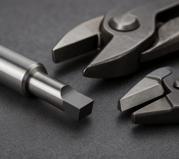
Precision tools are critical to the semiconductor manufacturing process, ensuring high accuracy, efficiency, and reliability in every stage of production. These tools play a vital role in wafer processing, die bonding, wire bonding, and component handling, where even the slightest deviation can impact product quality.
Many of these tools are designed with advanced materials such as carbide, tungsten, and ceramics to withstand the rigorous demands of semiconductor fabrication. Below are some of the most essential precision tools used in the industry.
1. Carbide Tips for Die Bonding & Component Handling
Carbide tips are extensively used in pick-up tools for die bonding and component handling in semiconductor assembly. Their high wear resistance and durability make them ideal for repeated use in high-precision environments.
Key Benefits of Carbide Tips:
✔ High Wear Resistance – Extends tool lifespan, reducing replacement frequency.
✔ Precision Handling – Ensures stable positioning of microchips and wafers.
✔ Minimal Contamination – Prevents particle buildup, maintaining process cleanliness.
Carbide-tipped tools are widely used in wafer processing, chip placement, and semiconductor packaging, ensuring accuracy and efficiency.
2. Ejector Pins & Needles for Molded Component Removal
Ejector pins and needles help remove semiconductor components from molds and dies after manufacturing. These tools are designed to prevent damage to delicate parts while ensuring smooth and precise ejection.
Differences Between Ejector Pins & Ejector Needles:
✔ Ejector Pins – Thicker and more rigid, suitable for standard ejection processes.
✔ Ejector Needles – Thinner and finer, designed for delicate semiconductor components that require gentle handling.
Made from hardened steel or carbide, these tools provide high durability and precision, minimizing the risk of component defects.
3. Epoxy Stamping Tools for Die Attach Processes
Epoxy stamping tools are used in die attach applications, ensuring precise epoxy dispensing for bonding semiconductor components. Proper application of epoxy minimizes waste and enhances bonding strength.
Why Epoxy Stamping Tools Are Important:
✔ Accurate Dispensing – Ensures uniform application, reducing material waste.
✔ Customizable Sizes – Adaptable for various semiconductor die bonding applications.
✔ Strong Adhesion – Enhances durability and reliability of bonded components.
These tools improve bonding precision, helping manufacturers achieve higher semiconductor assembly quality.
4. Wafer Probes & Probe Needles for Electrical Testing
Wafer probes and probe needles are essential for testing semiconductor wafers before packaging. These tools ensure that each semiconductor chip meets performance and reliability standards before further processing.
Features of Wafer Probes & Probe Needles:
✔ High-Precision Contact – Enables accurate electrical signal transmission.
✔ Made from Tungsten or Carbide – Ensures durability and resistance to wear.
✔ Used in Automated Test Equipment (ATE) – Enhances efficiency in semiconductor quality control.
By identifying defects early, these probes help reduce production waste and improve semiconductor reliability.
5. Capillaries for Wire Bonding
Capillaries guide bonding wires during semiconductor packaging, ensuring precise electrical connections between the die and substrate.
Importance of High-Precision Capillaries:
✔ Ensures Accurate Wire Placement – Prevents connectivity issues.
✔ Made from Ceramic, Carbide, or Synthetic Sapphire – Provides durability and precision.
✔ Used in Ball and Wedge Bonding – Supports different wire bonding techniques.
High-quality capillaries enhance semiconductor reliability by ensuring secure and precise wire bonds.
6. Dicing Blades for Wafer Cutting
Dicing blades are used to cut semiconductor wafers into individual dies with minimal material loss. These blades must be ultra-precise to avoid damaging delicate semiconductor components.
Features of Dicing Blades:
✔ Made from Diamond or Carbide-Coated Materials – Enables clean and precise cutting.
✔ Ensures High Precision – Reduces chipping and defects in diced wafers.
✔ Enhances Material Efficiency – Minimizes waste, improving yield rates.
Precision dicing blades help semiconductor manufacturers achieve higher throughput and better product quality.
7. Pick-and-Place Nozzles for Component Handling
Pick-and-place nozzles are used in automated semiconductor assembly to handle small components with accuracy and consistency.
Why Pick-and-Place Nozzles Matter:
✔ Customizable with Carbide Tips – Reduces wear and prevents contamination.
✔ Ensures Precise Placement – Enhances the accuracy of microchip positioning.
✔ Supports High-Speed Manufacturing – Boosts efficiency in automated assembly lines.
With increasing demand for miniaturized semiconductor devices, pick-and-place nozzles play a crucial role in efficient precision handling.
8. Bonding Tools for Wire Bonding (Wedge & Ball Bonding)
Bonding tools are used for wire bonding, ensuring secure and precise interconnections between semiconductor components.
Types of Bonding Tools:
✔ Wedge Bonding Tools – Used for ribbon and wedge bonding techniques.
✔ Ball Bonding Tools – Designed for ball bonding applications.
Made from tungsten carbide or titanium carbide, these tools provide high durability and precision, ensuring reliable semiconductor packaging.
9. Vacuum Tweezers for Safe Component Handling
Vacuum tweezers allow semiconductor manufacturers to handle fragile components with minimal contact, reducing the risk of electrostatic discharge (ESD) damage.
Benefits of Vacuum Tweezers:
✔ Non-Damaging Handling – Prevents scratches and contamination.
✔ Anti-Static Tips – Protects sensitive semiconductor components.
✔ Used in Wafer Handling & Packaging – Ensures safe and clean transfers.
These tools are particularly useful for ultra-thin wafers and delicate semiconductor components.
10. Wafer Handling End Effectors for Automated Transport
Wafer handling end effectors are robotic arms used to transport silicon wafers during semiconductor production.
Features of Wafer Handling End Effectors:
✔ Made from Ceramic or Carbon-Reinforced Composites – Prevents contamination.
✔ Ensures Non-Contact Handling – Reduces the risk of wafer breakage.
✔ Supports Automated Manufacturing – Enhances efficiency and precision.
With the growing use of automation in semiconductor fabrication, wafer handling end effectors help maintain process integrity and consistency.
Conclusion
Precision tools play a crucial role in semiconductor manufacturing, ensuring high accuracy, durability, and efficiency at every stage of production. From wafer handling and die bonding to wire bonding and dicing, these tools contribute to higher yields, reduced defects, and improved reliability.
Many of these tools feature carbide tips and advanced materials, offering enhanced wear resistance and performance for demanding semiconductor applications. As semiconductor technology continues to advance, the need for high-precision tooling solutions will only grow.
Would you like more details on specific precision tools for semiconductor applications? Let us know!