Key Takeaways
- Die bonding defects can significantly impact device reliability, especially in high-performance and high-power semiconductor applications.
- Most defects originate from process inconsistencies, including material handling, placement accuracy, and bonding conditions.
- Precision tooling, process control, and inspection systems are critical in preventing defects and ensuring consistent semiconductor packaging quality.
What causes a semiconductor device to fail even when the chip itself is perfectly designed?
In many cases, the issue lies not in fabrication, but in the die bonding process—a critical step that determines how securely and efficiently a die is attached within a package.
Die bonding, also known as die attach, is essential for ensuring mechanical stability, thermal performance, and electrical reliability. However, this process is highly sensitive to variations in materials, equipment, and environmental conditions. Even minor inconsistencies can introduce defects that compromise product quality.
Understanding the common defects in die bonding and how to prevent them is essential for manufacturers aiming to improve yield, reduce failure rates, and maintain consistent production standards.
What Is Die Bonding?
Die bonding is the process of attaching a semiconductor die to a substrate, leadframe, or package base using materials such as epoxy adhesives, solder, or sintered compounds.
This step is fundamental because it:
- Anchors the die mechanically
- Enables heat dissipation
- Supports electrical connectivity (in some configurations)
- Prepares the device for subsequent processes such as wire bonding or encapsulation
Given its importance, any defect at this stage can propagate through the entire assembly process.
Why Die Bonding Defects Matter
Defects in die bonding can lead to:
- Reduced thermal conductivity
- Mechanical instability
- Electrical performance degradation
- Premature device failure
In industries such as automotive, aerospace, and power electronics, these failures can have serious consequences. Therefore, identifying and eliminating defects early is critical.
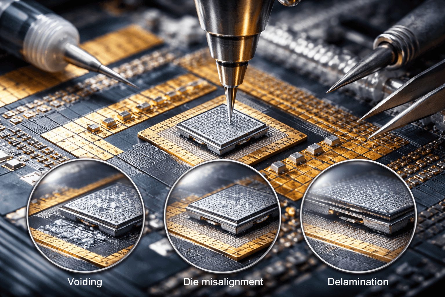
Common Defects in Die Bonding
1. Voiding
Description
Voids are air pockets or gaps trapped within the bonding material between the die and substrate.
Causes
- Inconsistent adhesive dispensing
- Improper curing profiles
- Contamination or moisture
Impact
- Reduced thermal conductivity
- Localised overheating
- Reduced reliability
Prevention
- Optimise dispensing parameters and material viscosity
- Use vacuum-assisted processes if required
- Ensure proper curing profiles and environmental control
2. Die Misalignment
Description
The die is not positioned correctly on the substrate or leadframe.
Causes
- Inaccurate pick-and-place systems
- Poor fixture design
- Operator or calibration errors
Impact
- Electrical connection issues
- Assembly failures in subsequent processes
- Reduced package integrity
Prevention
- Use high-precision placement systems
- Regularly calibrate equipment
- Implement alignment verification systems
3. Delamination
Description
Separation between the die and substrate or within the bonding layer.
Causes
- Poor adhesion
- Surface contamination
- Thermal mismatch between materials
Impact
- Mechanical failure
- Increased thermal resistance
- Long-term reliability issues
Prevention
- Ensure proper surface cleaning and preparation
- Select compatible materials
- Control thermal cycling conditions
4. Non-Uniform Bond Line Thickness (BLT)
Description
Inconsistent thickness of the bonding layer across the die.
Causes
- Uneven adhesive application
- Improper placement force
- Tooling inconsistencies
Impact
- Uneven stress distribution
- Reduced thermal performance
- Increased risk of delamination
Prevention
- Control dispensing volume precisely
- Use precision tooling to ensure uniform force distribution
- Monitor BLT during process validation
5. Die Tilt
Description
The die is tilted instead of sitting flat on the substrate.
Causes
- Uneven adhesive distribution
- Improper placement force or angle
- Tool misalignment
Impact
- Poor electrical connections
- Mechanical stress concentration
- Reduced reliability
Prevention
- Ensure uniform material application
- Maintain proper tool alignment
- Use flatness inspection systems
6. Excessive Adhesive Bleed-Out
Description
Adhesive spreads beyond the intended bonding area.
Causes
- Over-dispensing
- Low viscosity materials
- Incorrect placement pressure
Impact
- Contamination of surrounding areas
- Interference with wire bonding
- Cosmetic defects
Prevention
- Optimise dispensing volume and viscosity
- Fine-tune placement force
- Use controlled dispensing systems
7. Cracking or Die Damage
Description
Physical damage to the die during bonding.
Causes
- Excessive force during placement
- Improper tooling design
- Thermal stress
Impact
- Immediate device failure
- Reduced yield
Prevention
- Use precision-controlled force application
- Ensure tooling is designed for the die size and material
- Monitor stress conditions during bonding
Root Causes of Die Bonding Defects
Most defects can be traced back to a few core issues:
Process Variability
Inconsistent parameters such as temperature, pressure, or curing time can lead to defects.
Material Issues
Incorrect material selection or improper handling can affect bonding performance.
Equipment Limitations
Outdated or poorly calibrated equipment can introduce variability.
Tooling Precision
Inadequate or worn tooling can result in misalignment, uneven force, or inconsistent bonding.
The Role of Precision Tooling in Defect Prevention
For semiconductor manufacturers, precision tooling is a key factor in reducing die bonding defects.
High-quality tooling enables:
- Accurate die placement and alignment
- Controlled force application
- Consistent bond line thickness
- Improved repeatability across production runs
In advanced semiconductor packaging, tooling is not just a support component—it directly influences process stability and yield performance.
Best Practices to Prevent Die Bonding Defects
1. Optimise Process Parameters
- Standardise temperature, pressure, and curing profiles
- Monitor and adjust parameters regularly
2. Maintain Equipment Calibration
- Perform routine calibration
- Replace worn components
3. Improve Material Handling
- Store materials under recommended conditions
- Avoid contamination and moisture exposure
4. Implement Advanced Inspection
- Use X-ray and acoustic imaging
- Detect internal defects early
5. Invest in Precision Tooling
- Use tooling designed for tight tolerances
- Ensure consistent performance across high-volume production
Quality Control and Testing
To ensure die bonding integrity, manufacturers rely on:
- X-ray inspection for void detection
- Scanning Acoustic Microscopy (SAM) for delamination analysis
- Shear testing for bond strength evaluation
- Thermal cycling tests for long-term reliability
Accurate testing also depends on precision test tools, ensuring reliable and repeatable measurements.
Emerging Trends in Die Bonding
As semiconductor technology advances, defect prevention strategies are evolving:
- Automation and AI-driven inspection for defect detection
- Advanced materials with improved thermal performance
- Miniaturisation requiring tighter tolerances
- High-power applications demanding better heat dissipation
These trends further emphasise the importance of precision, consistency, and advanced tooling solutions.
Conclusion
Die bonding is a critical step in semiconductor packaging, and defects at this stage can significantly impact device performance and reliability. From voiding and misalignment to delamination and die damage, each defect has specific causes and consequences.
Preventing these issues requires a combination of process control, material optimisation, equipment calibration, and precision tooling. By addressing these factors, manufacturers can improve yield, enhance reliability, and maintain consistent production quality.
Final Thoughts & Next Steps
If your organisation is experiencing challenges in die bonding quality, it may be time to evaluate your process from a precision standpoint.
- Are your tools delivering consistent alignment and force control?
- Is your process stable across different production batches?
- Are defects being detected early enough to prevent downstream issues?
Working with experienced providers of precision tooling solutions for semiconductor applications can help minimise defects, improve yield, and strengthen long-term product reliability.

