Key Takeaways
- Die attach is a precision-critical step that directly impacts semiconductor reliability, thermal performance, and package integrity.
- Material selection and process control must align with application requirements, especially in high-power and advanced packaging environments.
- Precision tooling and process consistency are essential to minimise defects such as voiding, misalignment, and delamination.
What ensures a semiconductor device remains structurally stable and thermally efficient throughout its lifecycle?
While chip design often takes centre stage, the die attach process is a foundational step that determines how well a device performs in real-world conditions.
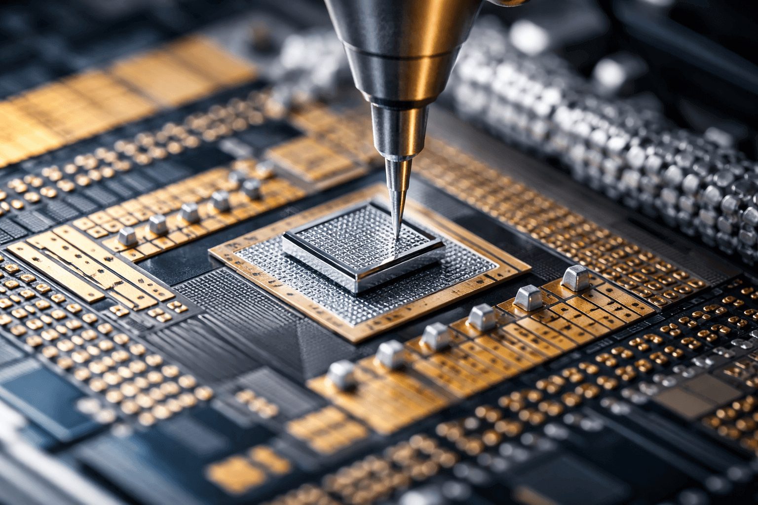
In semiconductor packaging, die attach involves bonding a silicon die onto a substrate or leadframe using specialised materials and highly controlled processes. As devices become more compact and performance-driven, the need for high-precision die placement, controlled bonding conditions, and reliable interconnect integrity becomes increasingly critical.
For manufacturers, achieving consistent results in die attach is not only about materials—it also depends heavily on precision tooling, equipment accuracy, and process repeatability.
What Is Die Attach?
Die attach is the process of mounting a semiconductor die onto a package substrate or leadframe using a bonding medium such as adhesive, solder, or sintered material. It is typically performed after wafer dicing and before wire bonding or encapsulation.
Why Die Attach Matters
The die attach process plays a multi-functional role:
- Mechanical stability: Ensures the die remains securely positioned during subsequent processes
- Thermal management: Enables efficient heat dissipation from the active device
- Electrical performance: Supports conductivity in certain package designs
- Process reliability: Reduces risk of defects during assembly and operation
In high-performance electronics, even slight inconsistencies at this stage can compromise the entire device.
The Role of Precision in Die Attach
Die attach is inherently a precision-driven process, where micrometre-level variations can influence performance outcomes.
Critical aspects include:
- Accurate die placement and alignment
- Controlled bond line thickness (BLT)
- Uniform material distribution (dispensing or film application)
- Stable force and temperature application during bonding
This is where precision-engineered tooling and fixtures play a crucial role. High-quality tooling ensures:
- Repeatable placement accuracy
- Consistent pressure distribution
- Minimal process variation across batches
Without proper tooling, even advanced materials and equipment may fail to deliver consistent results.
Types of Die Attach Materials
1. Epoxy Adhesives
Epoxy adhesives are widely used in standard semiconductor applications due to their versatility and ease of processing. They offer good adhesion and are generally cost-effective, making them suitable for high-volume manufacturing.
However, they typically have lower thermal conductivity compared to solder-based materials, which may limit their use in high-power or high-heat applications.
2. Solder Die Attach
Solder die attach uses metallic alloys such as SnAg or AuSn and is commonly applied in high-power and high-temperature environments. This method provides excellent thermal and electrical conductivity, along with a strong mechanical bond.
However, it requires higher processing temperatures and tighter process control, making precision tooling and thermal management essential.
3. Eutectic Bonding
Eutectic bonding involves melting a specific alloy at a defined temperature to create a highly reliable bond, often used in demanding applications such as automotive and aerospace electronics.
t delivers precise and robust interconnections but requires strict control of temperature profiles and alignment accuracy throughout the process.
4. Sintered Materials (e.g., Silver Sintering)
Sintered materials, particularly silver sintering, are increasingly used in advanced packaging and power electronics. They offer exceptionally high thermal conductivity and long-term reliability.
However, the process requires controlled pressure, temperature, and specialised tooling to ensure uniform bonding and avoid defects.
Step-by-Step Die Attach Process
1. Die Preparation
The wafer is diced into individual dies, which are then cleaned and inspected to ensure surface integrity.
2. Material Application
Adhesive or bonding material is applied through dispensing, printing, or film lamination. Precision in volume and placement is critical to avoid voiding or overflow.
3. Die Placement
The die is positioned onto the substrate using pick-and-place systems. High-precision alignment tools ensure accurate placement within tight tolerances.
4. Bonding or Curing
Depending on the material used:
- Adhesives are cured (thermal or UV)
- Solder undergoes reflow
- Sintering applies heat and pressure
Consistent force application is essential for uniform bonding.
5. Inspection
Inspection methods such as X-ray or acoustic imaging are used to detect voids, misalignment, or delamination.
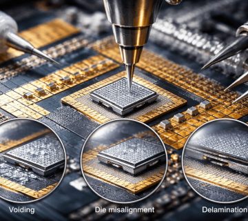
Common Challenges in Die Attach
Voiding
Air gaps within the bonding layer reduce thermal performance and reliability. This is often linked to inconsistent material application or improper process parameters.
Die Misalignment
Even slight positional errors can affect electrical connectivity and package performance. Precision placement tooling is critical to minimise this risk.
Delamination
Poor adhesion between die and substrate can occur due to contamination or incompatible materials.
Thermal Mismatch
Differences in thermal expansion between materials can introduce stress, especially in high-power applications.
How Precision Tooling Supports Die Attach Quality
For semiconductor manufacturers, achieving consistent die attach results depends heavily on tooling accuracy and durability.
Precision tooling contributes to:
- Consistent shear and bonding force application
- Accurate die positioning and alignment
- Stable process repeatability across high-volume production
- Reduced defect rates and improved yield
In advanced packaging environments, tooling is no longer just a supporting component—it is a critical enabler of process control and product reliability.
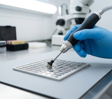
Quality Control and Testing
To ensure die attach integrity, manufacturers rely on:
- X-ray inspection for internal defects
- Scanning Acoustic Microscopy (SAM) for delamination detection
- Shear testing to evaluate bond strength
- Thermal cycling tests to assess long-term durability
Reliable testing outcomes also depend on precision test tooling, which ensures accurate force application and measurement consistency.
Emerging Trends in Die Attach
The semiconductor industry is evolving rapidly, and die attach processes are advancing alongside it:
- Miniaturisation requires tighter placement tolerances
- High-power devices demand superior thermal management
- Advanced packaging (2.5D/3D) increases process complexity
- Automation and smart manufacturing enhance precision and repeatability
These trends further highlight the growing importance of high-precision tooling solutions in semiconductor assembly.
Conclusion
The die attach process is a critical step in semiconductor packaging, directly influencing device performance, thermal efficiency, and long-term reliability. While material selection and process parameters are important, precision in execution is what ultimately determines success.
From die placement to bonding and inspection, every stage benefits from accurate, consistent, and well-engineered tooling. As semiconductor technologies continue to advance, the demand for precision-driven processes will only increase.
Final Thoughts & Next Steps
If you are involved in semiconductor manufacturing, evaluating your die attach process from a precision and tooling perspective can unlock meaningful improvements.
- Are your current tools delivering consistent alignment and force control?
- Is your process optimised for repeatability at scale?
- Are you minimising defects through precise application and inspection?
Partnering with experienced providers of precision tooling solutions for semiconductor applications can help enhance process stability, improve yield, and support long-term product reliability.
